Intel has updated the roadmap: on the horizon 2-nm and 1.4-nm process technology
During the event, the International Electron Devices Meeting (IEDM), ASML CEO Martin van den Brink spoke about his company’s plans for the next ten years. ASML is a manufacturer of photolithographic equipment for the microelectronic industry, which produces silicon wafers. One of the main customers of ASML is Intel.

Mr. van den Brink showed his slide, which was based on one of Intel’s September materials. Perhaps one of the most interesting news from the presentation is the fact that Intel is working hard to implement its plans to return the two-year production cycle known as Tick-Tuck.
The slide titled “In Moore, We Trust” (Intel believes in Moore’s law – approx. Author) talks about Intel’s plans for the future. In particular, each technological node will have several iterations for improvement. For example, the 7-nm process technology, in addition to the first option, will then be offered in 7 nm + and 7 nm ++ variations with increased energy efficiency and frequency potential.
No less interesting, the “twice-improved” manufacturing process will be fully compatible with the next-generation unit (for example, 7nm ++ and 5nm). This means that the architecture created under the 5-nm standard can easily be adapted to 7 nm ++ in case of problems with the development of new technologies.
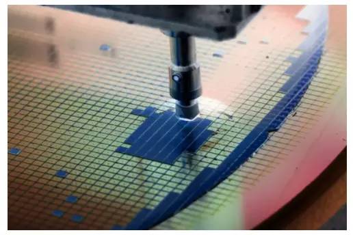
Intel is also developing new nodes that it plans to release in ten years. The crowning point of current plans is the 1.4-nm standard, which may be released in 2029. It is assumed that this manufacturing process will have a density of 1.6 billion transistors per square millimeter. For comparison, early Broadwell chips at 14 nanometers could boast a density of 37.5 million transistors per mm².